Features
- Войдите или зарегистрируйтесь, чтобы отправлять комментарии
 Ελληνικά
 Français
The LPC4350-DB1, LPC4357-DB1 and LPC1850-DB1 development boards differs by the assembled microcontroller. All other features are the same.
The basic modification of the development board contains:
- The NXP LPC series microcontroller (LPC4350-FET256, LPC4357-FET256 or LPC1850-FET256)
- High-speed USB 2.0 Host/Device/OTG interface (with USB mini-B connector)
- 10/100 Ethernet Port with on-board PHY
- 16MBit on-board NOR Flash
- 20-pin ARM standard JTAG connector
- 4 user push buttons, RESET button and 4 LEDs
- Boot select jumpers
The development boards have soldering options for the following components:
- External SDRAM (the 64 Mbit SDRAM is assembled at LPCXXXX-DB1-B and LPCXXXX-DB1-C board modifications)
- Real-Time Clock (RTC) crystal and power supply
- 10-pin 1.27mm (0.05 inch) Cortex Debug Connector
- 20-pin 1.27mm (0.05 inch) Cortex Debug + ETM Connector
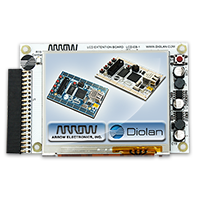
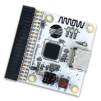
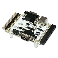
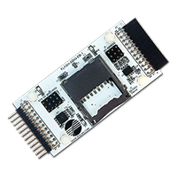
The functionality of the development board can be broaden with a wide range of extension boards:
 |
|
 |
HDMI/DVI Extension Board |
 |
RS232, RS485, CAN Bus and Full Speed USB Extension Board |
 |
SDIO/SD Card + I2C/SPI Memories Extension Board |
Английский
